Electronics is my passion
Sections
Unijunction transistor consists of N-type semiconductor bar with P-type region doped in the middle. The single P-N junction formed between these two layers accounts for the terminology unijunction.
![]()
The terminal which is connected to the P-type region is called emitter terminal. Silicon bar at its end has two ohmic contacts to which two terminals, base-1 and base-2 are connected. Therefore UJT is a unijunction three terminal device. In a unijunction transistor, the emitter is heavily doped while the N-region is lightly doped, so the resistance between the base terminals is relatively high.
Normally, base-2 is doped positively with respect to base1. If no voltage is applied at the emitter, extremely small current flows from base-2 to base-1.When a trigger voltage is applied at emitter, emitter-base junction is forward biased and a very large current will flow from emitter to Base-1. Both currents add together, which would create a larger output current. Device is not symmetrical since, emitter junction is usually located closer to base-2 than base-1. Therefore, the resistance between emitter and base-1 is larger than the resistance between emitter and base-2.
With a small constructional difference we can make complementary unijunction transistor. A complementary UJT is obtained by reversing the process involved in UJT as P-type base with N-type emitter terminal. A complementary UJT has exactly same characteristics as that of a conventional UJT, except for the polarities of voltage and current.
Consider, no voltage is applied at the emitter of the transistor and base-2 is positive with respect to base-1. Since the emitter is located nearer to base-2, more than half of Voltage across bases (VBB) appears between the emitter and base-1. The voltage between emitter and base-1, reverse bias P-N junction, and the emitter current is cut off. Only a small leakage current flows from base-2 to emitter due to minority carriers.
The P-N junction becomes forward biased, when the input voltage to the emitter increases. During this time, holes moves from P-region into the N-region. As base-2 is relatively positive when compared to base-1, the holes are attracted towards base-1 terminal and are repelled from base-1. Density of holes is more near base-1 region and results in the decrease of resistance in this section of the bar.
With this decrease in resistance, the voltage drop across the region also decrease, cause the emitter diode to be more heavily forward biased. Therefore forward current is increased, and consequently more charge carriers are injected causing further reduction in the resistance of the lower region. Thus the emitter current goes on increasing until it is limited by the emitter power supply. UJT can be turned off by a negative pulse applied to the emitter, the P-N junction is reverse biased and the emitter current is cut off.
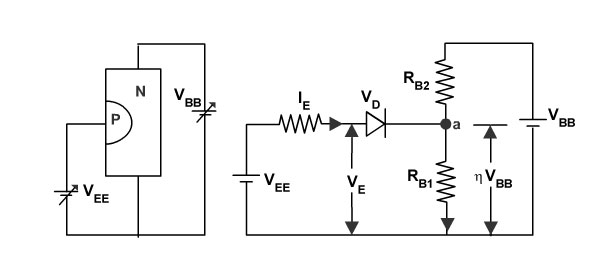
From the figure voltage required to forward bias P-N junction can be given by Vp
VP = η VBB + VD
Where η = RB1/ (RB1 + RB2)
VD = forward voltage drop across silicon diode
When input positive voltage to the emitter is less than VP, the P-N junction remains reverse biased and the emitter current is practically zero. If input voltage is increased above VPP-N junction is forward biased and emitter current starts flowing from emitter to base 1.

The figure shows the relation between emitter voltage and emitter current of a UJT for a constant voltage across bases. Initially, when no voltage is applied at the emitter, P-N junction is reverse biased. Now current in the device is only due to the flow of minority carriers. When input voltage is increased, leakage current is reduced and at a point, where voltage across the P-N junction is zero, then the current through the device is also reduced to zero. If the input voltage is further increased, at VP, emitter-base junction is forward biased.
Since the resistance of the device is dropped at this point, voltage across emitter base region is also reduced. This is the negative resistance portion of the curve where increase in IE, decreases VE. As shown in the figure, emitter current is continuously increased until it is limited by emitter power supply.


Sections


Copyright © 2024 Mepits - Designed By Digiora

